Author Affiliations
Abstract
1 Institute of Functional Nano and Soft Materials (FUNSOM), Jiangsu Key Laboratory for Carbon-Based Functional Materials and Devices, and Collaborative Innovation Center of Suzhou Nano Science and Technology, Soochow University, Suzhou 215123, China
2 Department of Materials Science and Engineering, Monash University, Clayton 3800, Australia
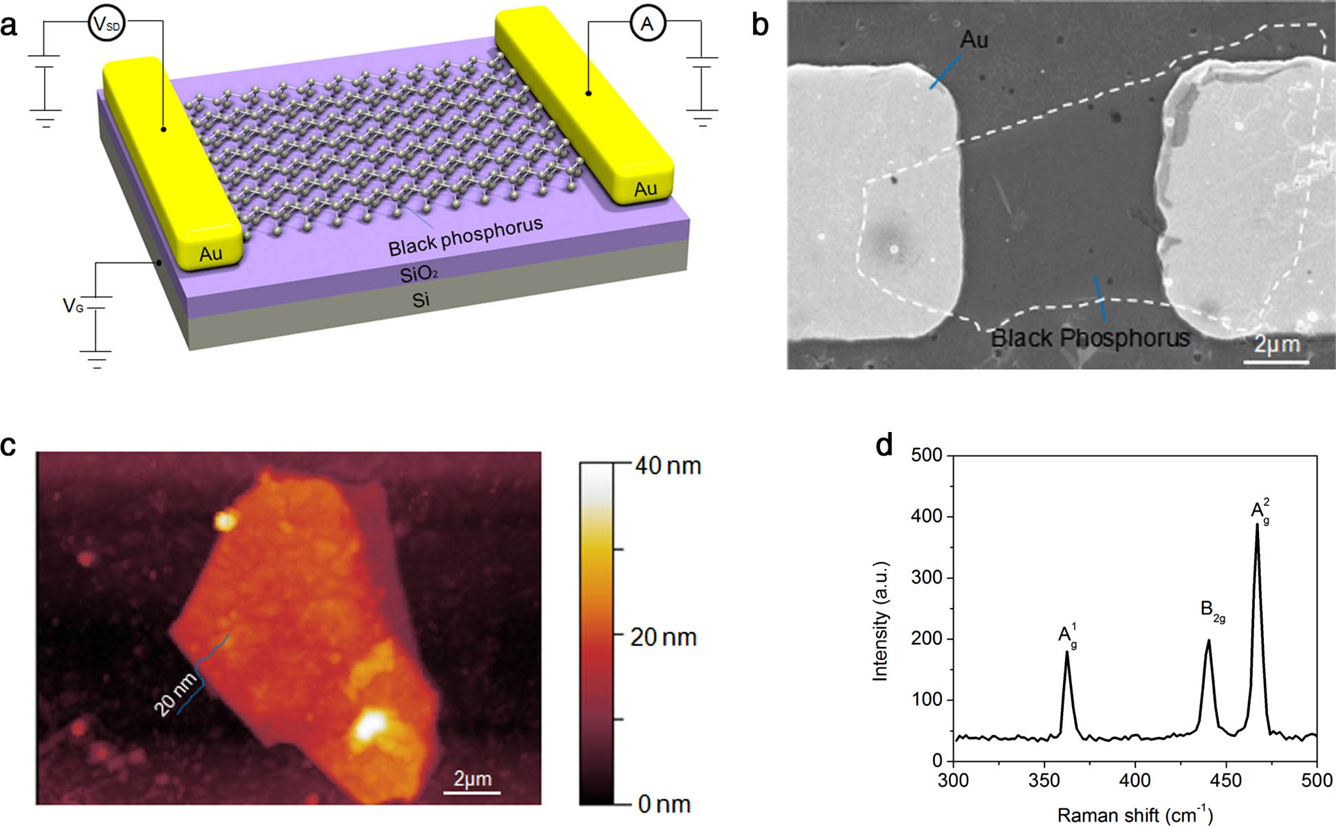
Black phosphorus (BP) is a promising material for ultrafast and broadband photodetection because of its narrow bandgap from 0.35 eV (bulk) to 1.8 eV (monolayer) and high carrier mobility. Although photodetectors based on BP with different configurations have been reported, high photosensitivity was mostly observed in the visible range. A highly efficient BP-based infrared photodetector operated in the telecom spectral range, especially at 1550 nm, has not been demonstrated. Here, we report a Schottky-type photodetector based on thin BP flakes, operating in a broad spectral range from visible (635 nm) to infrared (1550 nm). A responsivity as high as 230 A·W 1 was achieved at 1550 nm with a source-drain bias of 1 V. The rise time is 4.8 ms, and the fall time is 6.8 ms. Under light illumination and external bias, the Schottky barrier between the BP and metal was reduced, leading to efficient photocurrent extraction. The unprecedented performance of the BP photodetector indicates intriguing potential for sensing, imaging, and optical communication.
040.5160 Photodetectors 160.1890 Detector materials Chinese Optics Letters
2018, 16(2): 020002
1 华中科技大学 光学与电子信息学院, 武汉 430074
2 烽火通信科技股份有限公司, 武汉430074
为了在某些应急情况下无源传输声音信号, 采用基于光纤迈克尔逊干涉仪原理光纤声音传感的方法结合了收音弹性盘片和光纤粘接的工艺设计, 使用3×3耦合器相位解调方法对传感信号进行相位解调, 实现了一种新型光纤声音传感器系统。给出了干涉仪3路输出信号相位差的表达式, 利用最小二乘法拟合求出干涉仪3路输出信号的平均相位差, 取得了仿真与实际测试数据。经过测试, 该系统可以准确有效地还原出设计带宽内的声音信号。结果表明, 该光纤声音传感器系统适用于电磁恶劣等应急环境中, 验证了该设计方案的可行性。
传感器技术 3×3耦合器 相位差 解调 光纤 声音传感器 sensor technique 3×3 coupler phase difference demodulation fiber acoustic sensor

Author Affiliations
Abstract
1 Institute of Functional Nano and Soft Materials (FUNSOM), Jiangsu Key Laboratory for Carbon-Based Functional Materials and Devices, and Collaborative Innovation Center of Suzhou Nano Science and Technology, Soochow University, Suzhou 215123, China
2 Department of Materials Engineering, Monash University, Clayton, Victoria 3800, Australia
Atomically thin MoS2 films have attracted significant attention due to excellent electrical and optical properties. The development of device applications demands the production of large-area thin film which is still an obstacle. In this work we developed a facile method to directly grow large-area MoS2 thin film on SiO2 substrate via ambient pressure chemical vapor deposition method. The characterizations by spectroscopy and electron microscopy reveal that the as-grown MoS2 film is mainly bilayer and trilayer with high quality. Back-gate field-effect transistor based on such MoS2 thin film shows carrier mobility up to 3.4 cm2 V?1 s?1 and on/off ratio of 105. The large-area atomically thin MoS2 prepared in this work has the potential for wide optoelectronic and photonic device applications.
Materials and process characterization Materials and process characterization Spectral properties Spectral properties Thin film devices and applications Thin film devices and applications Thin films Thin films other properties other properties Photonics Research
2015, 3(4): 04000110


